
To solve the problem of 3D stacking and high-density anomalies, Colin R&D launches new sedimentation equipment
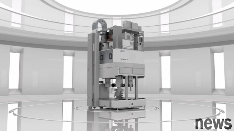
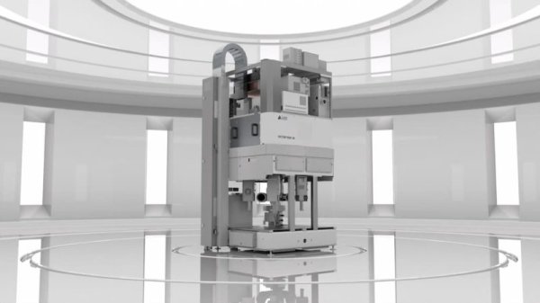
Lam Research today (10th) released the breakthrough sedimentation equipment VECTOR® TEOS 3D to solve the key advanced packaging problems in chip manufacturing required for next-generation artificial intelligence (AI) and high-performance computing (HPC) applications.
Colin R&D pointed out that TEOS 3D is designed to solve the key challenges in 3D stacking and high-density heterogeneity integration, adopts specialized cylindrical crystal round chip transmission solutions and innovative dielectric deposition technology, and enhances monitoring capabilities with the help of Colin R&D Equipment Intelligence technology, which can achieve ultra-thick and uniform inter-chip dielectric filling. At present, TEOS 3D has been put into use in the world's leading logical chips and memory chips.
Sesha Varadarajan, senior vice president of Colin R&D Global Products Group, pointed out that VECTOR TEOS 3D can deposition the thickest and void-free inter-chip dielectric layer-filled film in the industry, and can be customized according to the high difficulty requirements of advanced chip stacking integration solutions, and can be used even in ultra-high stress and high curved wafers. The differential atomic level innovation provided by this solution can help chip manufacturers break through the limitations of Morrow's law and move towards the AI era.
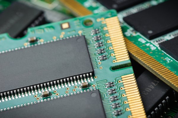
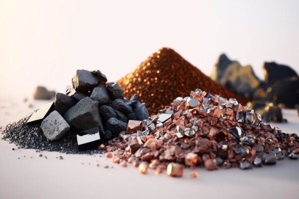
The explosive growth of artificial intelligence promotes the market to support the new component demands that are increasingly burdensome for large data work. Chip manufacturers are adopting advanced 3D packaging technology to integrate multiple chips into a chiplet architecture to realize AI computing power. By combining the memory and processing unit tighter and optimized circuit circuits, small wafer designs can increase processing speed and integrate higher efficiency in smaller sizes. However, as the stack height of the small wafer becomes more complex, a series of new manufacturing challenges arise, stress during the process may cause the wafer to twist or bend, and cracks and voids in the film may cause defects and reduce yields.
Colin Research and Development pointed out that TEOS 3D overcomes many key challenges in advanced packaging production and can accurately and reliably handle heavy, high-curved crystal flakes. It has a dedicated dielectric film with a nano-level precision of up to 60 microns between wafers and has the ability to expand the film with a deposition thickness of over 100 microns. This type of film provides key structure, heat learning and mechanical strength support to prevent common packaging failure problems such as layer structure disconnection.
In addition, TEOS 3D also supports Colin's unique mercury circular rolling technology and optimized mercury circular rolling design, which can provide excellent stability when processing thick crystal circles, and even surface-to-end crystal rounding can achieve uniform thin film deposition.
Extended reading: Aim at the challenge of advanced packaging! ERS Big Show Heat and Songkong Control Latest Solutions One of the keys to technological breakthroughs in GAA and CFET! ASM: Epictal technology has become an important role in advanced process