
TEK-ELECTRIC Activation and Development SoW-X Advanced Packaging, Production of High-Performance Data Center AI Chip
 According to
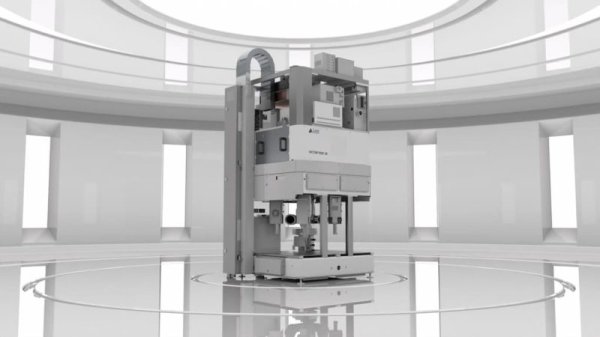
 PC Gamer, TEK announced that it will start the next-generation system-on-Wafer (SoW) packaging and development, named "SoW-X". It will make the market central processor (CPU) and graphics processor (GPU) chip surfaces look insignificant, bringing a subversive change to the data center and artificial intelligence (AI) field that pursues extreme computing capabilities.
Smart phones, wearable devices, mobile game machines, desktop computers, servers, and large data center equipment can see the processor, making the chips different in size. The current processors in high-level personal computers, whether AMD's Ryzen 9 9950X3D or Intel Core Ultra 9 285K processors, all use multiple chiplets, which is the technology of integrating and packaging multiple chips into a large processor. Telco's SoW-X technology is an advanced reality of this chip integration concept.
Compared with existing technology, SoW-X shows amazing scale and integration. Traditional chip packaging technicians typically install three to four small dies on substrates of about 7,000 mm². However, the coverage area of SoW-X chip packaging technology will be increased by 10 to 15 times, and even the entire 12-inch wafer round is required. One of the most eye-catching advances is the integration of more key components in the same wafer. Telco's first generation SoW packaging only installs processed grains into the wafer, and the new version of SoW-X can directly contain high-frequency wide memory (HBM) chips. This breakthrough integration technology represents no need to rely on the expensive, and complex external interconnects connect memory and processors, greatly simplifying the system design and improving efficiency.
To demonstrate the scale of SoW-X, even the large MI300X processor currently used by AMD for AI applications is unusually small in front of SoW-X. In fact, AMD's MI300X is an engineering miracle itself, as it contains 20 chips and dies, including four large I/O-based dies, eight CNDA 3 GPUs, and eight HBM modules, and Telco's SoW-X has the potential to multiply its size by ten times.
This large SoW-X product cannot be easily installed into existing interface slots. Since all dies are mounted on the same wafer, the wafer must be additionally plugged with multilayer structure to effectively dissipate heat, provide power, and transmit data inside the system. Therefore, although the crystals themselves are thin and sophisticated objects, once they are packaged with SoW-X, they become large, heavy and huge equipment. Therefore, SoW-X's main application scenarios will be locked in super-large AI data centers. In these environments with extremely high requirements for computing density, how to insert the most processing capabilities in the smallest space is the key to maximizing the available space inside the data center equipment. In this way, SoW-X is not only to create larger and better processors, it also pushes Moore% Law to a new peak.
In addition to pursuing absolute computing performance, SoW-X also brings significant improvements in energy efficiency. By placing as many components on the same substrate as possible, power consumption can be greatly reduced. Although Telco points out that the total power consumption of SoW-X will be as high as 17,000 watts, its performance-per-watt ratio is 65% higher than the traditional data center set that connects all components through a PCIe interface, which represents the ability of SoW-X to utilize energy more efficiently while providing the same, or even higher computing power.
SoW-X may seem far away for broad game players and ordinary family users. However, TEK will gradually be transferred to its daily packaging products through the knowledge and experience accumulated by the SoW-X system development and delivery. This means that future mobile phones, desktop CPUs and display cards will benefit from this, whether they currently use die or chip stacking technology, or when the actual limit on the number of single die transistors is reached at the stage.
Taiwan Electric estimates that SoW-X will only be in 2027. The cost of production is very high at a time, and only a few specific customers can afford it. The world of technology has also triggered the industry's thinking about the future direction of chip development, that is, will the crystal circle need to become larger after SoW-X? Or we will see the development of system-on-wafer-on-wafer to continue to promote the pursuit of stronger processing capabilities.
Although transistor sizes may not be reduced significantly, it is certain that future processors will become much larger. Taiwan Power continues to make breakthroughs in chip technology, and ultimately there is no need to choose partners, just wait patiently, because all customers will come to the door in the end. This will also enable SoW-X to once again consolidate its global semiconductor manufacturing leadership position in the context of Taiwan Electric's expected profits to exceed US$5 billion in 2025.