
Challenge 6 nm, power card advanced process market
UMC, the world's fourth largest large-scale crystal foundry manufacturer, is estimating the 6-nanometer process, thereby expanding the high-level chip market and seeking new growth dynamics. Sources pointed out that the United Nations Corporation is exploring the possibility of further expanding cooperation with Intel, planning to extend from the existing 12-nanometer cooperation base to 6 nanometers. In the future, both parties will not rule out further development of factory cooperation in Arizona.
6 Nano is an advanced process and is mainly used in AI accelerators, wireless communications and vehicle chips. The process still has a clear difference from previous generations. 7 nanometers are the last generation before EUV lithography, and DUV multiple exposure technology is widely used for detailed etching; while 6 nanometers are regarded as the key point for formal introduction to EUV mask machines.
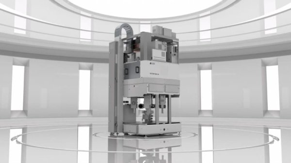
Whether to purchase EUV equipment becomes a key decision on whether the connection is entering the 6-nanometer process. EUV mask machines have a unit price of up to US$180 million to US$40 million, with a delivery time of more than one year, and need to be equipped with basic facilities such as highly clean rooms and professional maintenance. If you choose to use DUV with multiple exposures for 6-nanometer production, not only will the process be longer, but the yield may also decline significantly, which will create a challenge for the OEM model, which is known as high yield. In addition, the 6-nanometer width is smaller, and the difficulty of process control and defect rate management is also relatively improved.
Currently, the industry is leading the industry in the industry for the OEM industry, and continues to advance to advanced stages such as Amy. Only a few of those with 6-7 nanometer processing capabilities include Samsung and SMIC. Japanese OEM factory Rapidus chooses to skip this stage and directly invest in the 2nm process to develop.
Industry estimates that the total capital expenditure may be as high as US$5 billion for building a 6-nanometer line with a monthly capacity of 20,000 pieces of wafers. Whether the Telecom can successfully enter this field depends on whether it has sufficient customer support investment. Joint Financial Manager Liu Qidong said that if the company decides to enter the army of 6 nanometers, it will adopt the "asset light quantification" strategy to seek strategic partners to jointly cope with risks and avoid bearing the overall equipment and production energy pressure.
Taiwan’s No. 2 chipmaker UMC eyes entering cutting-edge race Extended reading: Telecom: Cooperation with Intel is one of the most important projects, 2027 mass production