
Select the subsidence, low temperature epitaxial super key! ASM comprehensively lays out new materials and solutions to fight against GAA and CFET problems
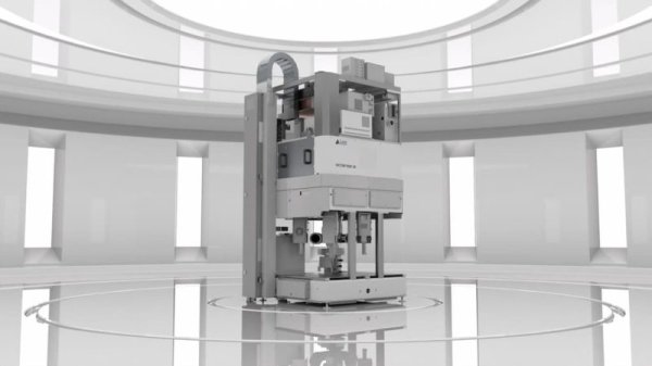
With the expected end-of-year production of NTF 2 nanometers, the Amy era will officially enter the second half of next year (2026). The micro-condensation of wafers has reached the physical limit, and Atomic Layer Deposition (simplified by ALD) has become one of the key technologies for extending Morrow's law and semiconductor slight reduction. In this regard, "New Science and Technology News" specially visited Glen Wilk, Vice President of Technology ASM, a Dutch semiconductor manufacturing equipment manufacturer, to help readers understand the importance of ALD in minimizing process.
Why is ALD so important? What is the difference with CVD and PVD?One of the main characteristics of ALD is layer-by-layer deposition atoms, which is a thin film processing technology that can grow the material layer-by-layer. "You can imagine it as snow. Every time only one layer of snow falls, it can make the sediment very uniform and have good coverage." Wilk said that ALD technology can make the sediment settle along the edge, even at the bottom, side or above.
In contrast, PVD (physical air phase deposition) is a "straight line deposition", like an arrow, it can only fly along the shooting direction (straight line), so it cannot turn or settle at the bottom or corner. Therefore, the coverage ability of PVD is very limited and can only settle in one direction.
As for CVD (chemical gas phase deposition) is similar to ALD, but each deposition is not a single layer atom, but a multilayer atom. Although it has a certain covering ability and can subside to the concave angle, it is not as accurate as ALD. Wilk notes that CVD cannot do it especially when precise control is performed in special parts (such as the bottom and corners). Although it is faster, its accuracy is not as accurate as ALD.
▲ Schematic diagram of three subsidence methods: PVD, CVD, and ALD. (Source: National Institute of Experience)
When the process is below 2 nanometers, ALD technology faces three major challengesWith the development of GAA and 3D architectures, due to the higher depth and width ratio and the deeper and narrower grooves, the requirements for sedimentation coverage, precision and thickness control are higher. Wilk said some structures will have two different layers, requiring sedimentation at the top and bottom. When the two may meet in the middle, avoid "clogging". Take straws as an example. If the inside of the straw is tinted, it will easily get stuck in the front or inlet. In addition, the inside is thin and narrow, the material may be stacked above, making it difficult to penetrate deep into the bottom, so the thickness is uniform and the thickness is properly controlled, making it more difficult.
The second challenge is "Area Selective Deposition, briefly ASD". When traditionally performing ALD technology, it will accurately and cover everything, but now demand is shifting to deposition in specific areas of the wafer, so "selective deposition" and "local deposition" have become important technologies that can save continuous exposure and processing steps and thus reduce costs.
The third challenge is "Gap Fill". If the structure is filled, the traditional way will allow the two sides of the materials to meet in the middle and form a gap (Seam). After the etching or other processes are subsequently carried out, the gap may become larger and larger, which will eventually lead to cracking. The solution is to directly and completely fill the middle structure through "Seam-free gap fill" to avoid the two side materials colliding together to create gaps.
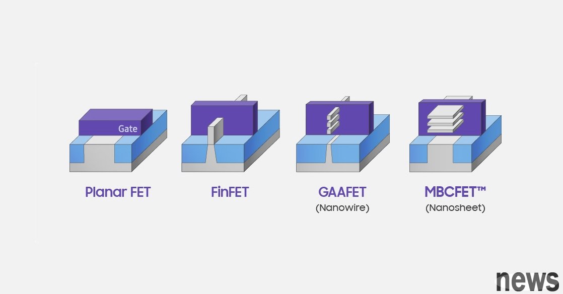
▲ CFET is the architecture on the right, and Samsung calls it MBCFET. (Source: Samsung)
These are challenges encountered in process micro-reduction. Wilk said that ASM has taken the lead in developing selective deposition (ASD) technology to help customers effectively solve advanced process challenges and improve process yield, component reliability and overall efficiency.
He also pointed out that if we move further to the CFET architecture, the ALD sediment will face more challenges, mainly in "low temperature sedimentation" and "optional sedimentation", which requires that it will be more stringent than GAA. The GAA challenge is a stacking layer, and CFETs stack one layer on top (i.e. stacking more than two layers). Just like building a high floor, how to achieve ultra-thin and even deposits from top to bottom and not generate gaps is a tricky problem.
In addition, CFETs have higher requirements for "low temperature deposition". In the past, the GAAFET architecture completed the process at the same time, so there was no problem with high temperature treatment; however, in the CFET architecture, it may be necessary to first manufacture the upper two layers and then carry out the lower two layers. However, when creating a new structure, high temperature is required, so that the completed old structure needs to face secondary high temperature, which may lead to damage or performance degradation. In addition, low temperature deposition will face the problem of elemental (such as carbon) destruction, which is also one of the challenges.
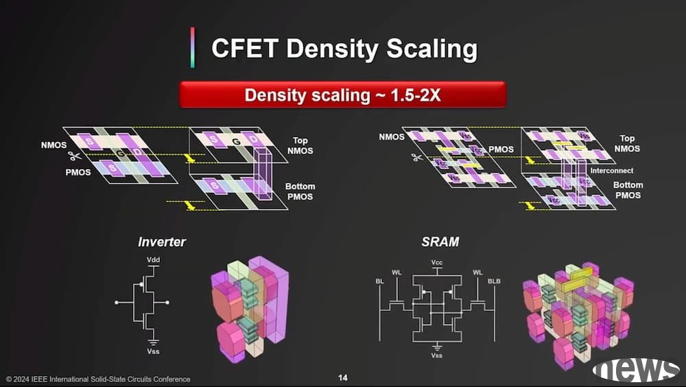
▲ From the above diagram, we can see that the grooves of the CFET architecture are deeper and narrower, and the sedimentation becomes tricky. (Source: TEK)
Chemical materials + hardware dual engine! ASM maintains ALD technology first with R&D teamsFor these challenges, ASM decided to find a new solution from materials and hardware. The company's corporate R&D department (Corporate R&D, briefly known as CRD) is responsible for developing advanced chemistry and process solutions. Some teams are located in Finland, working with Hersinki University, focusing mainly on material development, front-drive filtering and new path exploration; the other team cooperates with imec, the semiconductor research and development center, to further verify and simulate real environment testing.
These teams focus on studying new chemical reactions and new molecules to overcome the current sedimentation and blockage problems in specific areas. Wilk emphasizes that this requires a lot of new chemical formulas and innovations, which is also a unique advantage of ASM. In addition, as ALD's leading equipment supplier, ASM is also improving hardware design to match new chemical formulas, new molecules and new solutions, and effectively deliver chemical materials, so that they can achieve uniform coverage on the wafer while maintaining high efficiency and high speed.
"ASM purchased Finnish company Microchemistry as early as 1999, and ALD technology was invented by this company, and ASM also inherited this professional ability." Wilk believes that chemistry profession is one of the advantages of ASM. Being able to design corresponding hardware based on these chemical characteristics is another major advantage. "Through the combination of chemistry and hardware, it is the key to our always leading and core differentiation."
Comprehensive layout of new materials research and development, ASM aims at free gap filling, low temperature deposition and optional depositionASM research focuses include various types of gap-filling materials (silicon dioxide, silicon nitride), new gate stacking materials (work function metal and coupling), high-conductive heat-induced insulating layers, new contact materials, low-temperature epitaxial, silicon/silicon 3D DRAM epitaxial stacking, etc., and various films are also studied to solve the problems encountered by customers in the above process.
In addition, ASM also has a forward-looking department responsible for planning advanced technology, working closely with customers to explore potential solutions. Currently, the company is developing new materials, such as materials that can quickly guide heat and effectively dissipate heat, as well as new materials that still work well under extremely thin conditions (such as good insulating or conductive) to replace traditional thicker film layers. In addition, there are also many cooperations in driving before chemistry.
Through early cooperation with CRD, ASM can understand customer needs early and test solutions, and can continuously "test and learn" in a real environment, improve success rate, and promote new material layers to customers in advance. This is ASM's unique direction/enterprise level research and development, and it is also the company's differentiation advantage.
Wilk said that whether it is "unspark filling", "low temperature sedimentation" or "optional sedimentation", they are the most competitive areas at present. ASM has continued to develop chemical materials, combined with special hardware designs that match them, and can simplify process steps and greatly improve production capacity, further saving costs for customers.
In addition to ALD, epitaxial has also become the next major problem in the GAA eraIn Murray's law, the thickness of the transistor channel in the FinFET era is mainly determined by microfilm and etching; as technology evolves to the GAA structure, the silicon channel is directly grown from an epitaxial process with atomic precision.
Wilk said that when the GAA era, epitaxial would face two major challenges: "low temperature" and "grown nanosheets". The former is more difficult to control temperature due to the back power supply technology. In addition, the low temperature environment is prone to introduce complex quality, resulting in quality decline and becoming one of the key challenges. When building the channel process, epitaxials must alternately grow epitaxials to create multiple silicon channels separated from each other, which involves the problem of interface scalability.
In this regard, ASM also extends technology to the epitaxy field, emphasizing that the hardware design of the company's epitaxy equipment is different from that of competitors, and can achieve better control at low temperatures, while deposition of very uniform and high-quality films. In the Hybrid Bonding section of advanced packaging, ASM can provide hybrid bonding layers and related surface treatment technology. In addition, during the grain stacking integration process, heat must be dissipated through the extreme heat-conducting layer, which has become another major opportunity for ASM.
"The Taiwan team is very important to ASM!" ASM pointed out that Taiwan is the core leader of the global semiconductor industry and has always been the most indispensable part of the company's business development strategy. Last year, the Hsinchu office was launched to focus on R&D and customer support, and Tainan also has a training center responsible for supporting local needs and cultivating training centers for engineers from other countries. As for the global layout, ASM is currently mainly manufacturing bases in Singapore and the second manufacturing center is located in South Korea, with sufficient production capacity. In order to meet the current political situation, ASM will also add a new research and development unit location in the United States in 2027 to serve as a new tool for testing.
Extended reading: One of the keys to technological breakthroughs in GAA and CFET! ASM: Epictal technology has become an important role in advanced process ASML is actually the "three brothers"! A story of splitting up, accidentally revising the global semiconductor equipment pattern